Just as an essay begins with a blank sheet of paper, an electronic device begins with a blank slate as well. The electronics industry uses the acronyms PCB and PCBA interchangeably. However, the acronyms refer to products in two distinct phases of development.
The term PCB, or printed circuit board, refers to an inactive board that is ready to receive the components required to perform certain tasks and functionality. This connection is made during the assembly phase.
PCBA refers to a printed circuit board assembly or the process of attaching the essential electronic components to the PCB. It takes the blank slate of a printed circuit board and transforms it into the brains or functionality behind an electronic device.
What is a PCB?
A PCB starts as a flat board made of a non-conductive material, typically fiberglass or plastic. The choice of materials depends on the environmental conditions of the finished product and the components needed for the assembled PCB to perform its intended functions.
- Flexible PCBs are typically made of polyimide, allowing them to be bent, folded, or twisted to fit into tight spaces or conform to the shape of a particular device. Flexible PCBs are also used in applications where the board needs to withstand repeated flexing or bending, such as wearable technology and medical devices.
- Rigid PCBs, made of fiberglass, are the most common. They are durable and hold up well to mechanical stress. Rigid PCBs are often used in consumer electronics, industrial equipment, and automotive applications.
- Semi-rigid PCBs are made with a combination of flexible and rigid materials. They are used where the board needs to fit a specific form factor while requiring a certain level of rigidity to support the assembled components and environmental conditions. Semi-rigid PCBs are often used in high-density designs for applications such as aerospace and telecommunications.
Gerber, ODB++, or IPC 2581 design files are then used to define what gets “printed” on the circuit board. The board material is clad or coated with copper for conductivity, which is then etched to create circuitry pathways known as traces. Drill holes or other features needed for component placement are also added using CNC technology. The final PCB can vary in complexity depending on the needs of the final assembly.
- Single-sided PCBs are the simplest and most used type. The conductive material is on one side, while the components that make it perform a certain function are attached to the other side. Single-sided PCBs are usually used in low-density, low-cost applications.
- Double-sided PCBs have conductive material and components on both sides. This allows for a higher density of components for more complex circuit designs.
- Multi-layer PCBs consist of three or more layers of copper tracing and components, enabling high-density connectivity typically found in medical devices or other applications that require complex circuitry in a small size.
What is a PCBA?
A PCBA, or printed circuit board assembly, takes the next step in production using the PCB as the basis for applying the circuitry that will allow an electronic device to function. Using the engineering design files, resistors, capacitors, inductors, diodes, transistors, and integrated circuits are mounted to the PCB to create the final PCBA.
There are two types of prevalent mounting technologies: surface mount and through-hole technology.
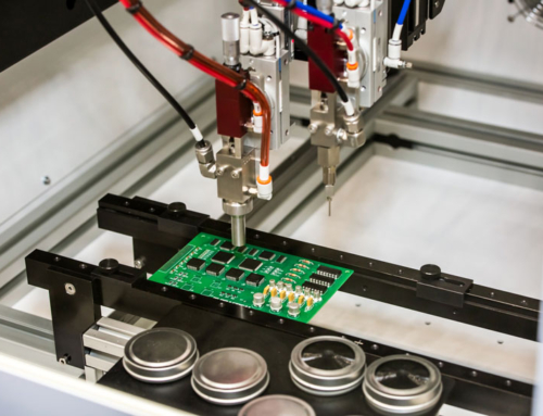
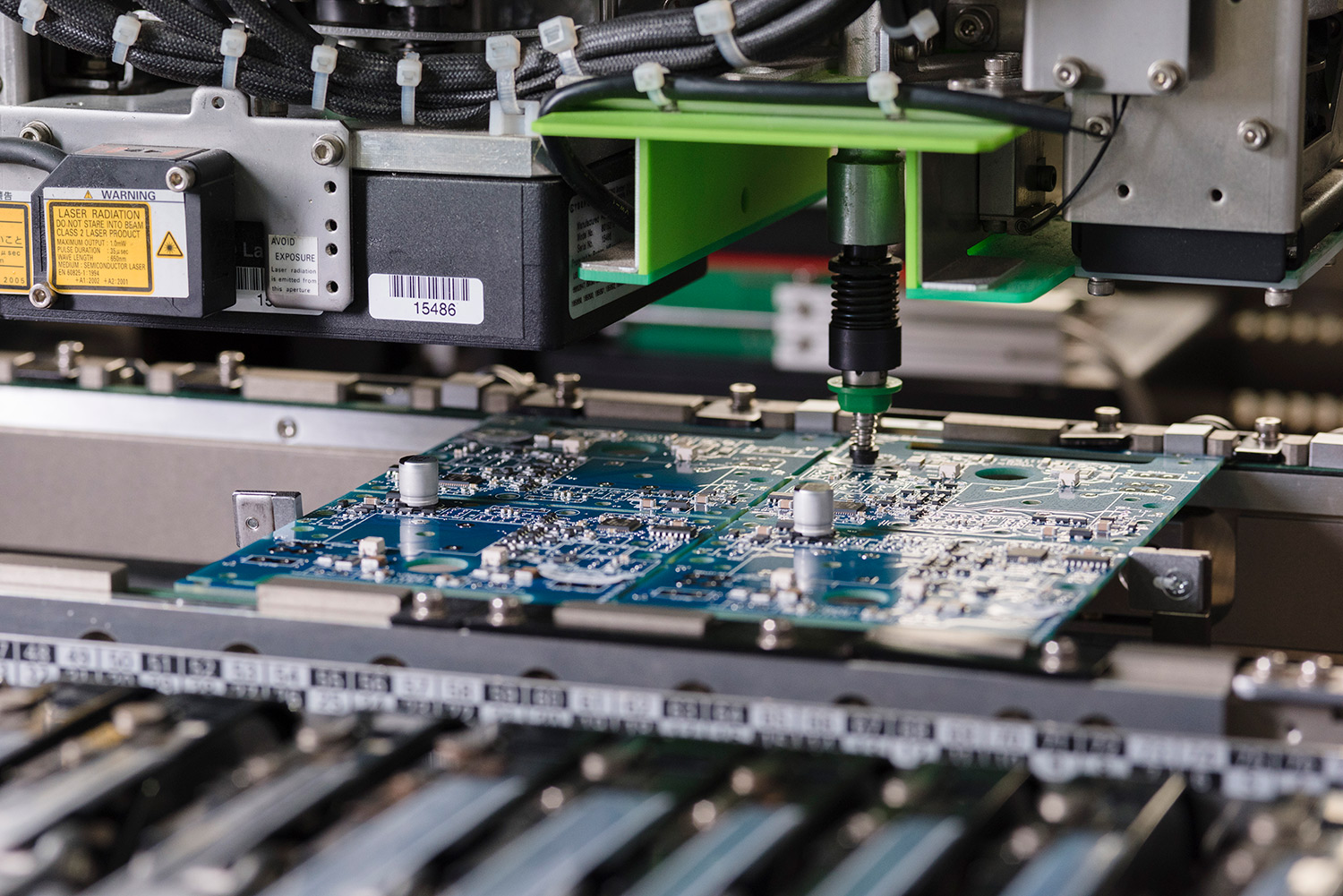
- Surface mount technology (SMT) is a multi-step process that includes solder paste application, component placement, reflow soldering, and inspection. Solder paste, a sticky mixture of tiny solder beads and flux, is first applied to the board’s solder pads using a stencil. A pick-and-place machine then precisely positions the designated components onto the board. After component placement, the board is heated in a reflow oven to melt the solder paste and secure the components into place.
- Through-hole technology (THT) is the process of inserting component leads into pre-drilled holes in a PCB. THT is typically done manually, although automated insertion machines are sometimes used for high-volume production. Once inserted, protruding leads are trimmed, and the components are secured to the board using wave or selective soldering. THT is slower than automated SMT but is still used in specialized applications requiring high mechanical strength.
PCBA validation and quality control
Various testing and inspection methods are used for SMT and THT assembly to ensure the printed circuit board assembly meets all design and functional specifications.
- Solder Paste Inspection (SPI) compares machine vision images of the solder points to the original design file to ensure paste deposits are within the specified tolerances.
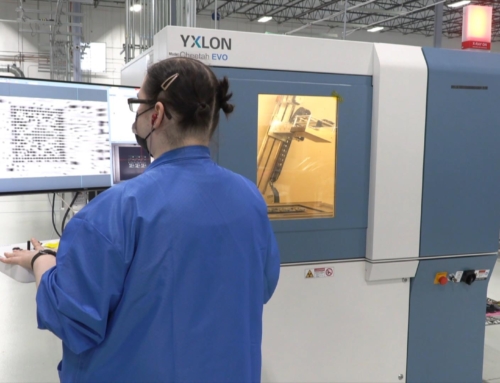
- Automated Optical Inspection (AOI) uses x-ray technology to ensure the structural integrity of a component or assembly. AOI detects voids in solder joints, cracks or fractures in components, or any other defects that may be difficult to see with traditional optical inspection methods. AOI is typically used in conjunction with SPI to provide a more comprehensive quality control checkpoint.
- In-Circuit Testing (ICT) involves using specialized testing equipment designed to measure the electrical characteristics of individual components. ICT can detect a wide range of defects, including missing components, incorrect component values, short circuits, and open circuits.
- Functional Testing (FCT) typically uses purpose-built test fixtures to simulate normal operating conditions for the PCBA. Depending on the product application, FCT can include hardware, software, firmware, and user interface testing.
Bring your project to life with the right PCBA manufacturer
To summarize, PCBs and PCBAs represent distinct phases within electronics manufacturing. An electronic device cannot function with a PCB alone. The assembly and insertion of circuitry that transforms it into a PCBA is like the “breath of life” that enables an electronic device to function.
A fully integrated PCBA manufacturer helps companies get to market faster by offering comprehensive design engineering, prototyping, manufacturing, supply chain management, and quality control. CO-AX Technology provides all of these services, in addition to cable and harness assembly and turnkey box builds.
With fully scalable production at our state-of-the-art facility in Northeast Ohio, we are uniquely qualified to respond to our customers’ exacting needs. Contact us today for help with your new or transfer PCBA project.